

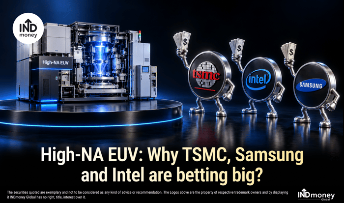
- What has changed in ASML’s High-NA EUV story?
- What is High-NA EUV lithography and why does it matter?
- Why do TSMC, Samsung and Intel have different adoption strategies?
- Why could larger photomasks improve High-NA economics?
- Can a more expensive chip machine lower manufacturing costs?
- What do ASML’s latest financial results reveal?
- How could High-NA strengthen ASML’s business?
- ASML stock valuation: How much growth is already priced in?
- What could weaken the High-NA investment case?
- What does ASML’s opportunity mean for Indian investors?
- What should investors watch next?
The next stage of the chip race will depend partly on whether a more advanced machine can make a working chip more cheaply. That is the commercial promise behind ASML’s High-NA EUV technology. TSMC, Samsung and Intel are backing it on different schedules, giving ASML a broader opportunity while leaving investors with a harder question: how much of that future is already reflected in its share price?
Let’s break down how High-NA EUV works, why the three chipmakers are adopting it at different speeds and what the latest developments mean for ASML’s earnings, valuation and Indian investors.
What has changed in ASML’s High-NA EUV story?
The important developments are the company announcements published on 8 September 2026. These set out different adoption plans and a shared effort to improve the technology’s longer-term economics.
| Company | Confirmed position | What investors should understand |
| Intel | Already using High-NA on selected layers for a subset of Panther Lake processors | Commercial use exists, but the entire product range has not switched |
| Samsung | Plans High-NA in high-volume DRAM manufacturing by 2028 | The dated commitment concerns memory manufacturing |
| TSMC | Intends to introduce High-NA in advanced-node high-volume manufacturing from 2030 | A production roadmap is clearer, although substantial adoption is still ahead |
| ASML and ecosystem partners | Target a larger-mask pilot line by 2031 and production-system readiness by 2033 | This is a subsequent productivity project rather than the start date for all High-NA use |
The schedules matter. Treating these announcements as an immediate wave of factory conversions would bring future revenue into the investment case too early. Equally, saying that High-NA remains purely experimental would overlook Intel’s existing production use.
Sources: ASML’s joint announcements with Intel, Samsung and TSMC, 8 September 2026; Samsung Semiconductor Global Newsroom; TSMC corporate newsroom.
What is High-NA EUV lithography and why does it matter?
Lithography transfers extremely small patterns onto a light-sensitive coating on a silicon wafer. Those patterns guide later manufacturing steps that build the chip’s structures. Think of a very sophisticated printing process repeated across the layers of a chip.
EUV stands for extreme ultraviolet. ASML’s EUV systems use light with a wavelength of 13.5 nanometres. High-NA retains that wavelength but improves the optical system’s ability to resolve fine details. NA means numerical aperture: broadly, a measure of how much light the optics can collect and use for imaging.
| Feature | Conventional EUV | High-NA EUV |
| ASML platform | NXE | EXE |
| Numerical aperture | 0.33 | 0.55 |
| Main change | Established EUV imaging | Finer imaging through larger, more advanced optics |
| Manufacturing opportunity | Multiple patterning where necessary | Potential to simplify difficult layers into fewer patterning steps |
ASML specifies 8 nm resolution for its EXE:5200B. This is a lithography specification, not a statement that the machine only makes chips marketed as “8 nm”. Manufacturing-node names and individual printed dimensions describe different things.
The financial attraction is process simplification. When a pattern is too difficult to produce in one exposure, manufacturers may split the work into additional patterning steps. Each extra step can consume equipment time, materials and manufacturing capacity.
A sharper imaging system can therefore be valuable even when it costs more. The relevant comparison is the cost of the complete manufacturing route and the number of usable chips it produces.
High-NA also brings a trade-off. With the current mask format, its exposure field is half the size of the NXE field. Large chip designs may require adjustments or stitching, which joins separately exposed portions of a pattern. That is why the mask project matters alongside improvements in resolution.
Why do TSMC, Samsung and Intel have different adoption strategies?
The three companies face a shared engineering problem but different commercial decisions. A manufacturing advance creates value only when it fits a company’s products, production schedule and economics.
TSMC: Adopt when the manufacturing case is ready
TSMC intends to begin High-NA high-volume manufacturing from 2030. Its announcement also expects more layers to require the technology as transistor architectures become more complex. It does not name a specific first node, so assigning the rollout to a particular future node would go beyond the release.
For a foundry, which manufactures chips designed by customers, the decision has several dimensions. A new process must deliver competitive cost, predictable production and sufficiently reliable output for customers to commit their designs. An earlier installation date alone does not establish an advantage across all those measures.
Our interpretation is that TSMC’s timing reflects the importance of introducing High-NA where it delivers a worthwhile manufacturing improvement. Waiting can preserve returns on existing tools while early collaboration keeps the next option available. The risk is waiting too long if competitors make the new process economically superior sooner.
Samsung: Improve the economics of memory manufacturing
Samsung’s dated commitment is to introduce High-NA in future DRAM high-volume manufacturing by 2028. It is also participating in the larger-photomask initiative. The announcement should not be rewritten as a promise that every Samsung foundry process will use High-NA by that date.
DRAM provides the working memory used in computing systems. For a memory manufacturer, the potential prize is producing usable memory capacity more efficiently. Denser patterns and a simpler process could help, but the investment must still earn its way through operating costs, yields and selling prices.
Our view is that a technological improvement is most financially valuable when it lowers cost per usable unit through the cycle. If a company adds expensive capacity just as memory prices weaken, technical progress can coexist with poor returns on capital. Investors should therefore assess manufacturing economics alongside the adoption date.
Intel: Turn early production experience into a repeatable advantage
Intel’s position is more advanced in demonstrated use. ASML’s July announcement confirmed High-NA on specific Intel 18A layers for a subset of Core Ultra Series 3 processors, known as Panther Lake. Those layers were dual-qualified, with reported yields matching the conventional NXE route.
In September, the companies reported more than one million wafers processed across tool certification, testing, research and production. That combined figure is not a count of commercial wafers shipped to customers.
Early experience can help a manufacturer learn how to operate equipment reliably, reduce interruptions and integrate new processes. Those lessons have potential value beyond the first products. However, the economic test remains whether they translate into competitive manufacturing and profitable customer demand.
Intel’s progress strengthens the evidence that High-NA can work in production. It does not independently establish the profitability of Intel’s entire foundry business or prove that its full process is superior to competing processes.
Why could larger photomasks improve High-NA economics?
A photomask contains the pattern that the lithography system projects onto the wafer. The proposed larger format is commonly described as a 12-inch mask; Intel’s announcement specifies a 6-by-12-inch format. It should not be confused with a 12-inch silicon wafer.
The objective is to increase productivity and address the stitching constraints associated with the current format. The industry is targeting a pilot line in 2031 and readiness for advanced-node production in 2033. High-NA can be used before this transition, as Intel’s existing work demonstrates.
The investment implication is that High-NA has more than one opportunity to improve its economics. Initial adoption can simplify selected layers. Later changes to the mask ecosystem could improve how efficiently manufacturers use the equipment.
That also creates execution risk. A common format requires coordination across equipment, materials, design tools and handling systems. An announced target is meaningful because it aligns the industry, but investors should wait for evidence of readiness before treating the later benefits as certain.
Can a more expensive chip machine lower manufacturing costs?
Yes, provided it reduces total cost per working chip. The machine’s purchase price is only one part of that calculation.
A useful framework is:
Cost per working chip = Total manufacturing cost per wafer ÷ Number of working chips from that wafer.
Total cost includes allocated equipment costs, maintenance, materials and the other processing steps. Working-chip output depends on both the number of possible chips and yield, which is the proportion that functions correctly.
Consider this deliberately simplified example. These are illustrative assumptions rather than ASML or customer disclosures.
| Assumption | Existing process | Successful High-NA transition | Difficult High-NA transition |
| All-in manufacturing cost per wafer | $20,000 | $21,000 | $21,000 |
| Potential chips per wafer | 600 | 600 | 600 |
| Yield | 80% | 88% | 75% |
| Working chips | 480 | 528 | 450 |
| Cost per working chip | $41.67 | $39.77 | $46.67 |
| Change against the existing process | — | 4.5% lower | 12.0% higher |
The successful case has a higher wafer cost but a lower cost per working chip because the improvement in output more than compensates. The difficult case shows how an expensive transition can destroy that benefit if yield disappoints. Holding chip count constant isolates the yield effect; an actual process comparison would also examine density, performance and the chip’s selling price.
Under these assumptions, yield must exceed 84% just to beat the existing unit cost. The calculation is $21,000 divided by 600 chips and then divided by the original $41.67 cost per working chip, using unrounded values.
This is the question investors should ask about each customer: what must improve to justify the incremental investment? Statements about resolution become financially meaningful when they answer that question.
What do ASML’s latest financial results reveal?
ASML’s latest published quarter at this article’s cutoff is Q2 2026. Its accounts are reported in euros. The figures below use the company’s US GAAP releases rather than converting them into dollars.
| Metric | Q2 2025 | Q2 2026 |
| Net sales | €7.692 billion | €9.326 billion |
| Gross margin | 53.7% | 54.0% |
| Operating margin | 34.6% | 37.1% |
| Net income | €2.290 billion | €2.918 billion |
| Basic earnings per share | €5.90 | €7.59 |
Revenue increased approximately 21.2% while net income rose 27.4%. Profit growing faster than sales is encouraging, although one quarter cannot establish a permanent trend. Gross margin is the amount left after production costs; operating margin also reflects expenses such as research and administration.
Source: ASML Q2 2026 investor presentation. Growth rates calculated from reported figures.
ASML also generated €2.762 billion in Installed Base Management sales, comprising service and field-option revenue. That represented approximately 29.6% of quarterly sales. Existing equipment therefore provides an important revenue stream alongside new systems, although upgrades and service activity can still fluctuate.
The July outlook called for 2026 sales of €43 billion–€45 billion and gross margin of 54%–56%. For Q3, management guided to €11 billion–€12 billion of sales. These are forecasts, not reported results.
The comparison base is €32.667 billion of sales in 2025. The latest annual guidance therefore implies approximately 31.6%–37.8% growth. That is a demanding expansion, which makes shipment execution and customer readiness relevant well before TSMC’s future High-NA ramp.
High-NA is also only part of ASML’s opportunity. In July, management outlined plans to expand conventional EUV and immersion DUV capacity. Investors should avoid assigning the company’s entire near-term growth outlook to the newest platform.
How could High-NA strengthen ASML’s business?
ASML is the sole commercial supplier of EUV lithography systems. That position makes it a common supplier to manufacturers competing for advanced-chip business. The next question is how much economic value it can retain as their production requirements change.
We see three mechanisms worth tracking. More production use can create demand for systems. A larger operational fleet can support service and upgrade work. Close involvement in customer process development can make ASML’s technology harder to replace within an established manufacturing workflow.
Those mechanisms should not be combined into an assumption of unlimited pricing power. Customers assess the economics of the whole factory. If a tool’s cost rises faster than the savings it enables, a manufacturer has a reason to delay adoption or extend an existing process.
An additional complication is that fewer patterning steps are good for customers but can change the number of exposures required. Equipment demand ultimately depends on wafer volumes, the layers assigned to each technology, effective throughput and utilisation. Multiplying the number of future factories by a headline machine price is too crude to value this opportunity.
Our assessment is that broader customer adoption improves the durability of ASML’s growth opportunity. Its financial scale will depend on how deeply High-NA enters production and how much value each system delivers over its operating life.
ASML stock valuation: How much growth is already priced in?
ASML’s US-listed shares closed at $1,743.94 on 25 September 2026. That is the latest completed regular US session available at this article’s morning cutoff on 28 September.
| Valuation reference | Reading used |
| US-listed closing share price | $1,743.94 |
| Approximate market capitalisation | About 660 - 670 Billion |
| Approximate trailing P/E | Around 55 times |
At roughly 55 times trailing earnings, investors are paying about $55 for each $1 of annual earnings. The implied earnings yield is around 1.8%, calculated as one divided by the multiple. This is not a dividend yield or a promised return.
Such a valuation can be supported by strong future growth, but it leaves the investment sensitive to both earnings delivery and the multiple investors accept later. A superior business can still generate disappointing stock returns if its purchase valuation requires too much success.
The following model starts at 55 times earnings and tests five-year outcomes. All growth rates and ending multiples are assumptions, not analyst consensus or price targets. It excludes dividends, taxes, fees and currency changes.
| Annual EPS growth for five years | P/E after five years | Cumulative share-price change | Annualised share-price return |
| 10% | 35 times | +2.5% | +0.5% |
| 15% | 40 times | +46.3% | +7.9% |
| 20% | 45 times | +103.6% | +15.3% |
| 20% | 55 times | +148.8% | +20.0% |
The calculation is: Ending price ÷ Starting price = (1 + annual EPS growth)⁵ × Ending P/E ÷ Starting P/E.
The first scenario is especially useful. Earnings grow materially, yet most of the benefit disappears because investors pay a smaller multiple at the end. In the second, 15% earnings growth becomes a share-price return below 8% a year.
If the multiple falls from 55 to 40 over five years, EPS must grow approximately 6.6% annually merely to keep the share price unchanged. That is the growth required to offset valuation compression before generating capital appreciation.
Our view is that ASML’s strategic position warrants serious attention, but the current valuation already demands substantial execution. The case needs a credible earnings path and a sensible ending valuation alongside confidence in High-NA.
What could weaken the High-NA investment case?
The biggest risks concern timing and economic returns. A technology can succeed eventually while disappointing shareholders who expected earlier growth.
Customer adoption could progress more slowly. Production targets depend on qualification and cost. Fewer initial layers or delayed factory ramps would reduce the pace of equipment demand even if customers remain committed to the technology.
Reliability and supporting infrastructure could constrain output. A factory earns from usable production. Better nominal specifications are insufficient if interruptions, materials or process integration prevent sustained output.
AI spending could become less profitable for customers. A manufacturer’s willingness to expand depends partly on demand for the chips it produces. If end customers earn less than expected on their infrastructure spending, capacity decisions can become more cautious.
Geopolitics can restrict the addressable market. Export controls are a material exposure for semiconductor equipment. Existing restrictions and any further changes can affect where ASML can sell or service technology, independently of customer demand.
The share-price multiple could fall before the business weakens. Investors may demand a lower valuation because expected growth slows or other investments become more attractive. The scenario table shows why that risk deserves separate attention from the technology itself.
What does ASML’s opportunity mean for Indian investors?
ASML offers Indian investors researching global technology stocks exposure to semiconductor manufacturing equipment. Its economics differ from those of a chip designer or a company operating chip factories, even when all benefit from the same end demand.
That distinction also matters for diversification. Owning several semiconductor-related companies may spread company-specific risk while retaining a common dependence on capital spending and advanced-chip demand. Investors should look through the different business names to the underlying drivers.
There is a direct Indian industrial connection. In May 2026, Tata Electronics and ASML announced an agreement covering lithography tools and support for the Dholera fab, together with talent and ecosystem development. The release describes a planned $11 billion facility and a technology portfolio including 28 nm and larger nodes.
That agreement does not announce an Indian High-NA deployment. It is also separate from the larger-mask initiative: the Dholera plant’s 300 mm wafer size does not mean it is using the proposed larger photomasks.
For anyone studying Indian semiconductor stocks, the practical lesson is to identify the actual activity a company performs and the contracts supporting it. Exposure to assembly, manufacturing equipment or chip design should not be treated as interchangeable.
Indian investors also experience currency effects when measuring overseas investments in rupees. As a purely illustrative calculation, a 10% dollar share-price gain combined with a 5% rise in the dollar against the rupee produces a 15.5% rupee return before costs and taxes: 1.10 × 1.05 − 1. If the dollar instead falls 5%, that same stock gain becomes 4.5%. Currency can help or hurt.
What should investors watch next?
The most useful updates will show whether technical progress is becoming repeatable financial progress.
| Evidence to monitor | Why it matters |
| Customer production qualification | Separates a working installation from a commercially usable process |
| High-NA use across more layers and products | Indicates whether adoption is broadening |
| Yield, availability and effective throughput | Tests the economics of actual production |
| ASML sales delivery, margins and cash generation | Shows whether demand is turning into profitable business |
| Larger-mask pilot progress | Tests the feasibility of the next productivity improvement |
| Earnings growth relative to the stock’s valuation | Determines whether business success can produce attractive investor returns |
No single announcement answers all these questions. The stronger case develops when technical readiness, customer adoption and financial delivery reinforce each other.
Our central conclusion is that the September commitments make High-NA a more credible long-term growth opportunity for ASML. The decisive evidence will be cheaper working chips for customers and sustained earnings growth for the equipment supplier. At an earnings multiple around the mid-50s, investors also need to judge how much of that progress the share price already anticipates.